Technical Documents
Specifications
Brand
Renesas ElectronicsProduct Type
Buffer
Maximum Input Frequency
105MHz
Maximum Propagation Delay Time
150ps
Mount Type
Surface
Package Type
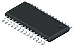
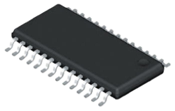
TSSOP
Pin Count
28
Minimum Supply Voltage
3.13V
Maximum Supply Voltage
3.46V
Minimum Operating Temperature
0°C
Maximum Operating Temperature
70°C
Length
9.7mm
Height
1mm
Standards/Approvals
PCIe Gen1 and Gen2
Series
9DB106
Automotive Standard
No
Product Details
The Renesas Electronics zero delay buffer supports PCIe Gen1 and Gen2 clocking requirements. The is driven by a differential SRC output pair from an IDT compliant main clock generator. It attenuates jitter on the input clock and has a selectable PLL bandwidth to maximize performance in systems with or without Spread spectrum clocking. An SMBus Interface allows control of the PLL bandwidth and bypass options, while 2 clock request pins make the suitable for Express card applications.

Ideate. Create. Collaborate
JOIN FOR FREE
No hidden fees!


Stock information temporarily unavailable.
55,813.20 MOP
27.907 MOP Each (On a Reel of 2000) (ex VAT)
2000
55,813.20 MOP
27.907 MOP Each (On a Reel of 2000) (ex VAT)
Stock information temporarily unavailable.
2000
| quantity | Unit price | Per Reel |
|---|---|---|
| 2000 - 8000 | 27.907 MOP | 55,813.22 MOP |
| 10000+ | 27.349 MOP | 54,697.08 MOP |
Ideate. Create. Collaborate
JOIN FOR FREE
No hidden fees!
Technical Documents
Specifications
Brand
Renesas ElectronicsProduct Type
Buffer
Maximum Input Frequency
105MHz
Maximum Propagation Delay Time
150ps
Mount Type
Surface
Package Type
TSSOP
Pin Count
28
Minimum Supply Voltage
3.13V
Maximum Supply Voltage
3.46V
Minimum Operating Temperature
0°C
Maximum Operating Temperature
70°C
Length
9.7mm
Height
1mm
Standards/Approvals
PCIe Gen1 and Gen2
Series
9DB106
Automotive Standard
No
Product Details
The Renesas Electronics zero delay buffer supports PCIe Gen1 and Gen2 clocking requirements. The is driven by a differential SRC output pair from an IDT compliant main clock generator. It attenuates jitter on the input clock and has a selectable PLL bandwidth to maximize performance in systems with or without Spread spectrum clocking. An SMBus Interface allows control of the PLL bandwidth and bypass options, while 2 clock request pins make the suitable for Express card applications.
Ideate. Create. Collaborate
JOIN FOR FREE
No hidden fees!