技術文件
規格
Brand
NexperiaProduct Type
Shift Register
Mount Type
Surface
Maximum Supply Voltage
6V
Minimum Operating Temperature
-40°C
Maximum Operating Temperature
125°C
Standards/Approvals
RoHS
產品詳情
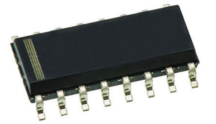
The 74HC4094, 74HCT4094 is an 8-bit serial-in/serial or parallel-out shift register with a storage register and 3-state outputs. Both the shift and storage register have separate clocks. The device features a serial input (D) and two serial outputs (QS1 and QS2) to enable cascading. Data is shifted on the LOW-to-HIGH transitions of the CP input. Data is available at QS1 on the LOW-to-HIGH transitions of the CP input to allow cascading when clock edges are fast. The same data is available at QS2 on the next HIGH-to-LOW transition of the CP input to allow cascading when clock edges are slow. The data in the shift register is transferred to the storage register when the STR input is HIGH. Data in the storage register appears at the outputs whenever the output enable input (OE) is HIGH.
暫時無法取得庫存資訊。
84.00 MOP
1.68 MOP Each (In a Tube of 50) (不含稅)
50
84.00 MOP
1.68 MOP Each (In a Tube of 50) (不含稅)
暫時無法取得庫存資訊。
50
| 數量 | 單價 | 每管子 |
|---|---|---|
| 50 - 50 | 1.68 MOP | 83.99 MOP |
| 100 - 200 | 1.636 MOP | 81.82 MOP |
| 250 - 450 | 1.597 MOP | 79.86 MOP |
| 500+ | 1.548 MOP | 77.39 MOP |
技術文件
規格
Brand
NexperiaProduct Type
Shift Register
Mount Type
Surface
Maximum Supply Voltage
6V
Minimum Operating Temperature
-40°C
Maximum Operating Temperature
125°C
Standards/Approvals
RoHS
產品詳情
The 74HC4094, 74HCT4094 is an 8-bit serial-in/serial or parallel-out shift register with a storage register and 3-state outputs. Both the shift and storage register have separate clocks. The device features a serial input (D) and two serial outputs (QS1 and QS2) to enable cascading. Data is shifted on the LOW-to-HIGH transitions of the CP input. Data is available at QS1 on the LOW-to-HIGH transitions of the CP input to allow cascading when clock edges are fast. The same data is available at QS2 on the next HIGH-to-LOW transition of the CP input to allow cascading when clock edges are slow. The data in the shift register is transferred to the storage register when the STR input is HIGH. Data in the storage register appears at the outputs whenever the output enable input (OE) is HIGH.